Emergen Research, a leading provider of market research solutions, is thrilled to announce the release of its highly anticipated collection of comprehensive market research content. This innovative offering aims to empower businesses across industries with valuable insights and data-driven strategies to drive growth and success.
We have recently released a 250-page report from Emergen Research that includes 194 tables and 189 charts and graphics. Those who need commercial, in-depth market assessments for the global Nanopatterning market, as well as a detailed market segment analysis, can find our new report valuable. Our recent study provides a thorough assessment of the whole regional and global market for Nanopatterning.
To increase market share, obtain a comprehensive financial analysis of the whole market and its various segments. It is clear that energy storage technology is rapidly expanding. Look at how you might take advantage of the current and future revenue-generating opportunities in this industry. Additionally, the research will assist you in making more effective strategic decisions, such as building growth strategies, strengthening competitor analysis, and increasing business productivity.
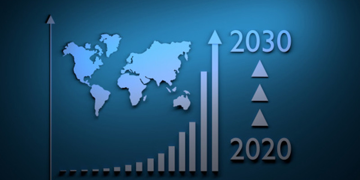
The global Nanopatterning Market was valued at approximately USD 2.4 billion in 2024 and is projected to reach nearly USD 8.9 billion by 2034, registering a CAGR of 13.7% over the forecast period. The Nanopatterning market growth is boosted by drivers such as the miniaturization of semiconductor chips, growth in demand for high-resolution patterning for advanced electronics, and growing applications in photonics, biotechnology, and quantum computing.
The shift toward sub-5nm chip architectures and heterogeneous integration is accelerating the need for precise nanopatterning tools capable of fabricating features at the atomic scale. Techniques such as nanoimprint lithography (NIL), extreme ultraviolet (EUV) lithography, and electron beam lithography (EBL) are becoming central to overcoming the limitations of traditional photolithography, enabling the production of denser, faster, and more power-efficient integrated circuits.
Top semiconductor foundries are heavily investing in next-generation lithography platforms to lead the chase for Moore's Law extension. Nanopatterning is now crucial in making critical dimension control possible on FinFETs, gate-all-around (GAA) FETs, and 3D NAND architectures. Concurrently, research laboratories and medtech innovators are taking advantage of nanopatterned surfaces for biosensing, DNA sequencing, and lab-on-chip diagnostics as a result of their capacity to control biological interactions on the nanoscale.
In the meantime, manufacturers are getting creative with new resist materials, directed self-assembly (DSA), and hybrid top-down/bottom-up methods to enhance throughput, decrease defect levels, and minimize cost per wafer. With expanding demand for ultra-high-density data storage, AR/VR optics, and next-generation photonic components, nanopatterning technology should be at the root of making the next generation of nano-enabled innovation possible.
Key Benefits for Stakeholders:
- The report provides an extensive analysis of the current and future trends in the global minimally invasive surgical systems market to elucidate the imminent investment pockets.
- A detailed analysis of the factors that drive and restrict the growth of the minimally invasive surgical systems market is provided.
- Extensive analysis of key segments demonstrates the types of energy devices, access equipment, and visualization & documentation systems used in minimally invasive surgeries.
- A comprehensive analysis of the geographical landscape provides detailed information about various regions across North America, Europe, Asia Pacific, Latin America, and Middle East & Africa.
- The report offers a competitive landscape of the minimally invasive surgical systems market to assist players to gain insights into the competition scenario. Key companies operating in the market are profiled to provide valuable insights.
Request Free Sample Copy (To Understand the Complete Structure of this Report [Summary + TOC]) @ https://www.emergenresearch.com/request-free-sample/148
The global Nanopatterning Market was valued at approximately USD 2.4 billion in 2024 and is projected to reach nearly USD 8.9 billion by 2034, registering a CAGR of 13.7% over the forecast period. The Nanopatterning market growth is boosted by drivers such as the miniaturization of semiconductor chips, growth in demand for high-resolution patterning for advanced electronics, and growing applications in photonics, biotechnology, and quantum computing.
The shift toward sub-5nm chip architectures and heterogeneous integration is accelerating the need for precise nanopatterning tools capable of fabricating features at the atomic scale. Techniques such as nanoimprint lithography (NIL), extreme ultraviolet (EUV) lithography, and electron beam lithography (EBL) are becoming central to overcoming the limitations of traditional photolithography, enabling the production of denser, faster, and more power-efficient integrated circuits.
Top semiconductor foundries are heavily investing in next-generation lithography platforms to lead the chase for Moore's Law extension. Nanopatterning is now crucial in making critical dimension control possible on FinFETs, gate-all-around (GAA) FETs, and 3D NAND architectures. Concurrently, research laboratories and medtech innovators are taking advantage of nanopatterned surfaces for biosensing, DNA sequencing, and lab-on-chip diagnostics as a result of their capacity to control biological interactions on the nanoscale.
In the meantime, manufacturers are getting creative with new resist materials, directed self-assembly (DSA), and hybrid top-down/bottom-up methods to enhance throughput, decrease defect levels, and minimize cost per wafer. With expanding demand for ultra-high-density data storage, AR/VR optics, and next-generation photonic components, nanopatterning technology should be at the root of making the next generation of nano-enabled innovation possible.
Competitive Landscape:
The latest study provides an insightful analysis of the broad competitive landscape of the global Nanopatterning market, emphasizing the key market rivals and their company profiles. A wide array of strategic initiatives, such as new business deals, mergers & acquisitions, collaborations, joint ventures, technological upgradation, and recent product launches, undertaken by these companies has been discussed in the report.
Miniaturization of Semiconductor Devices Driving Demand for High-Precision Nanopatterning Techniques
The primary driver propelling the Nanopatterning Market demand is the uncompromising miniaturization of semiconductor devices, particularly as the industry enters the sub-5nm node era. With increasing consumer demand for increasingly fast, power-efficient, and smaller electronic devices, the pressure on manufacturers to develop integrated circuits (ICs) with ultra-fine geometry and close line-width control is on the rise. Nanopatterning technologies, including nanoimprint lithography, electron beam lithography, and extreme ultraviolet (EUV) lithography, have become crucial in facilitating the manufacture of next-generation semiconductor architectures such as FinFETs, gate-all-around (GAA) transistors, and 3D NAND memory.
Conventional photolithography techniques are approaching their physical and economic boundaries, especially with regard to resolution and overlay precision. Nanopatterning provides the precision to define features below the sub-10nm scale yet preserve pattern fidelity over increasingly varied wafer topographies. This is important not just for logic and memory chips but also in developing applications like system-on-chip (SoC) and heterogeneous integration where multiple functionalities are integrated in a compact single footprint.
In addition, international semiconductor foundries like TSMC, Samsung, and Intel are increasing investment in next-generation nanopatterning equipment to improve yield and sustain Moore's Law. Spreading of AI accelerators, 5G baseband ICs, AR/VR CPUs, and edge computing chips is also increasing pressure on nanoscale lithography solutions that provide high resolution along with high throughput.
Apart from semiconductors, nanopatterning is also picking up traction in photonics, biosensors, and data storage, where nanoscale structuring of surfaces provides unprecedented manipulation of light, biology, and magnetic domains. With the technology foundation for future electronics and advanced materials, nanopatterning is emerging as a keystone of innovation in a rapidly nano-driven world.
Trends and Innovations
- Shift Toward EUV and Multi-Patterning Techniques: As semiconductor devices continue scaling below the 5nm node, chipmakers are increasingly turning towards extreme ultraviolet (EUV) lithography and multi-patterning methods. These technologies provide higher pattern resolution and fewer patterning steps, achieving tremendous improvements in throughput while minimizing edge placement error (EPE) for advanced logic and memory chips.
- Emergence of Nanoimprint Lithography (NIL) in Display and Photonics: NIL is coming into prominence in uses apart from semiconductors, especially in nano-structured optical films, metasurfaces, and bendable displays. Its cost savings, high throughput, and the capability to replicate sub-10nm features are broadening its application in AR/VR optics, antireflective coating, and biosensors.
- Hybrid Patterning Platforms Integrating E-Beam and Optical Lithography: To fill the gap between resolution and volume scalability, hybrid nanopatterning technologies are being developed. They integrate the accuracy of electron beam lithography with the speed of optical methods, providing tunable feature resolution for R&D and pilot-line production of advanced materials and 2.5D/3D packaging.
- Adoption of Directed Self-Assembly (DSA) for Sub-7nm Features: DSA is emerging as a viable alternative or supplement to standard lithography for the production of periodic nanostructures with unprecedented precision. Utilizing block copolymers, which spontaneously assemble into patterns at the nanoscale, DSA is being investigated for bit-patterned media, fin patterning, and contact hole shrink processes in volume manufacturing.
- Biocompatible Nanopatterning for Biomedical Devices: Biomedical applications of nanopatterning are growing exponentially. Scientists are employing nanopatterned surfaces to control cellular adhesion, tissue growth, and drug release kinetics. This is facilitating the development of implantable sensors, lab-on-a-chip diagnostics, and tissue engineering scaffolds with nano-engineered surface textures.
- AI-Powered Process Optimization and Defect Inspection: Machine learning algorithms and artificial intelligence are increasingly being incorporated into nanopatterning workflows to enable predictive process control, anomaly detection, and real-time defect classification. Such tools are enhancing yield, variability reduction, and more intelligent tool calibration in fabs.
Emergen Research is Offering a full report (Grab a Copy Now) @ https://www.emergenresearch.com/industry-report/nanopatterning-market
Market Segmentation:
The report bifurcates the Nanopatterning market on the basis of different product types, applications, end-user industries, and key regions of the world where the market has already established its presence. The report accurately offers insights into the supply-demand ratio and production and consumption volume of each segment.
Our goal at Emergen Research is to empower businesses with the knowledge and insights necessary to make informed decisions and thrive in today's dynamic business landscape. Our market research content is designed to equip professionals and organizations with comprehensive analyses, actionable recommendations, and a competitive edge to achieve their growth objectives.
Custom Requirements can be requested for this Report [Customization Available] @ https://www.emergenresearch.com/request-for-customization/148
The global Nanopatterning Market was valued at approximately USD 2.4 billion in 2024 and is projected to reach nearly USD 8.9 billion by 2034, registering a CAGR of 13.7% over the forecast period. The Nanopatterning market growth is boosted by drivers such as the miniaturization of semiconductor chips, growth in demand for high-resolution patterning for advanced electronics, and growing applications in photonics, biotechnology, and quantum computing.
The shift toward sub-5nm chip architectures and heterogeneous integration is accelerating the need for precise nanopatterning tools capable of fabricating features at the atomic scale. Techniques such as nanoimprint lithography (NIL), extreme ultraviolet (EUV) lithography, and electron beam lithography (EBL) are becoming central to overcoming the limitations of traditional photolithography, enabling the production of denser, faster, and more power-efficient integrated circuits.
Top semiconductor foundries are heavily investing in next-generation lithography platforms to lead the chase for Moore's Law extension. Nanopatterning is now crucial in making critical dimension control possible on FinFETs, gate-all-around (GAA) FETs, and 3D NAND architectures. Concurrently, research laboratories and medtech innovators are taking advantage of nanopatterned surfaces for biosensing, DNA sequencing, and lab-on-chip diagnostics as a result of their capacity to control biological interactions on the nanoscale.
In the meantime, manufacturers are getting creative with new resist materials, directed self-assembly (DSA), and hybrid top-down/bottom-up methods to enhance throughput, decrease defect levels, and minimize cost per wafer. With expanding demand for ultra-high-density data storage, AR/VR optics, and next-generation photonic components, nanopatterning technology should be at the root of making the next generation of nano-enabled innovation possible.
Target Audience of the Global Nanopatterning Market Report:
- Key Market Players
- Investors
- Venture capitalists
- Small- and medium-sized and large enterprises
- Third-party knowledge providers
- Value-Added Resellers (VARs)
- Global market producers, distributors, traders, and suppliers
- Research organizations, consulting companies, and various alliances interested in this sector
- Government bodies, independent regulatory authorities, and policymakers
Key features and benefits of Emergen Research's market research content include:
- Comprehensive Analysis: Each piece of content is meticulously researched and provides a detailed analysis of market trends, competitive landscape, consumer behavior, and emerging opportunities. Businesses can leverage this information to identify untapped markets, devise effective marketing strategies, and make data-driven decisions.
- Actionable Recommendations: The market research content provides practical insights and actionable recommendations to help businesses enhance their products, services, and overall customer experience. These recommendations are tailored to the specific needs and challenges of each industry, allowing companies to implement strategies that drive growth and profitability.
- Expert Insights: Emergen Research's team of industry experts and analysts contribute their in-depth knowledge and expertise to every piece of content. Their insights shed light on industry-specific challenges, best practices, and emerging trends, helping businesses stay ahead of the competition and seize new opportunities.
- Timely Updates: The market research content is regularly updated to reflect the latest market trends and dynamics. Subscribers will have access to the most up-to-date information, enabling them to adapt their strategies and stay relevant in today's rapidly evolving business environment.
The global Nanopatterning Market was valued at approximately USD 2.4 billion in 2024 and is projected to reach nearly USD 8.9 billion by 2034, registering a CAGR of 13.7% over the forecast period. The Nanopatterning market growth is boosted by drivers such as the miniaturization of semiconductor chips, growth in demand for high-resolution patterning for advanced electronics, and growing applications in photonics, biotechnology, and quantum computing.
The shift toward sub-5nm chip architectures and heterogeneous integration is accelerating the need for precise nanopatterning tools capable of fabricating features at the atomic scale. Techniques such as nanoimprint lithography (NIL), extreme ultraviolet (EUV) lithography, and electron beam lithography (EBL) are becoming central to overcoming the limitations of traditional photolithography, enabling the production of denser, faster, and more power-efficient integrated circuits.
Top semiconductor foundries are heavily investing in next-generation lithography platforms to lead the chase for Moore's Law extension. Nanopatterning is now crucial in making critical dimension control possible on FinFETs, gate-all-around (GAA) FETs, and 3D NAND architectures. Concurrently, research laboratories and medtech innovators are taking advantage of nanopatterned surfaces for biosensing, DNA sequencing, and lab-on-chip diagnostics as a result of their capacity to control biological interactions on the nanoscale.
In the meantime, manufacturers are getting creative with new resist materials, directed self-assembly (DSA), and hybrid top-down/bottom-up methods to enhance throughput, decrease defect levels, and minimize cost per wafer. With expanding demand for ultra-high-density data storage, AR/VR optics, and next-generation photonic components, nanopatterning technology should be at the root of making the next generation of nano-enabled innovation possible.
About Emergen Research
Emergen Research is a market research and consulting company that provides syndicated research reports, customized research reports, and consulting services. Our solutions purely focus on your purpose to locate, target, and analyze consumer behavior shifts across demographics, across industries, and help clients make smarter business decisions. We offer market intelligence studies ensuring relevant and fact-based research across multiple industries, including Healthcare, Touch Points, Chemicals, Types, and Energy.
Contact Us:
Eric Lee
Corporate Sales Specialist
Emergen Research | Web: https://www.emergenresearch.com/
Direct Line: +1 (604) 757-9756
E-mail: sales@emergenresearch.com